PicNic - yet another emulator/spyware for HF RFID
(c) Copyright by Tomas Rosa in 2008-2010, http://crypto.hyperlink.cz
Email to: tomas_dot_rosa (at) rb_dot_cz
This material can be freely used for an educational purpose only. Anyway, its usage can be a subject to a law regulation.
The author takes no responsibility for any direct/indirect damage or incident done by using the content of this page.
Last update: June 14th 2010
Page history
June 14th 2010: The idea of SAM-PicNic originally noted on April 6th 2010 (cf. bellow) is updated.
Juna 14th 2010: FakeUID 1.5-beta OpenCard Special Edition is added to the firmware section.
April 6th 2010: Idea on using NFC-WI/S2C interface of NXP chipset for attaching the PicNic module is described.
April 6th 2010: Crypto1 coprocessor status updated, FakeUID 1.4 released, FakeUID 1.5-beta released.
November 27th 2009: Note on PicNic enhanced by Crypto1 VHDL-based coprocessor added. Cf. bellow.
Abstract
Rather than a final construction, this is just an experimental kit addressed to anybody, who wants to play with e.g. MIFARE chip emulation etc. It has two main parts – HW module which is a simple microcontroller driven HF RFID transceiver and a particular SW module which does the particular job (fake UID sending, terminal spying, MIFARE hacking, etc.). The modules currently available in public are listed bellow. Of course, it is definitely up to you to build your own HW/SW modules basing on some of those already existing. Remember – this is a kit... it all started as a demo project for my students, then I decided to put it here - just for an inspiration.
The name PicNic itself explain the main design paradigm and also tells why I did construct „yet another emulator/spyware“. The word “Pic” comes from the name of the microcontroller family being used, while “Nic” comes from the Czech word for “Nothing”. So, PicNic = PIC and „Nothing else around it“. Thus, in opposite to the other designs available on the internet which often try to be as robust as possible, I searched for a minimal design possible. I do not say I have reached the absolute minimum, but I feel I am close enough.
The whole design is addressed to people with a moderate knowledge of radio electronics, PIC programming, and RFID technology.
Documentation
Rosa, T.: PicNic for HF RFID, Santa’s Crypto Get-together 2008, Rump Session presentation, Prague
Klima, V. and Rosa, T.: PicNic pro RFID-KV, Sdelovaci technika, 1/2009
(this article is in Czech, I hope I will find a time to translate it; nevertheless, the scheme and short notes presented bellow together with source code comments in assembler files should be enough to understand how it works and how to build it up)
HW design
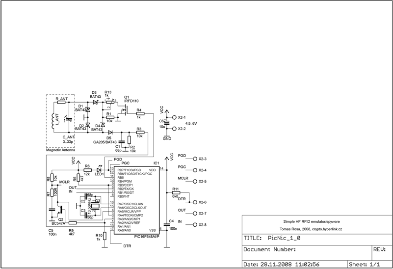
Note on the PIC clock source
The microcontroller oscillator is driven by X-tal with parallel resonant frequency at 13.56 MHz. We should use a parallel cut with a load capacitance approx. 30 pF. Using the same frequency as of the basic carrier, we can get easily synchronized with the RFID terminal on the very basic level of the instruction flow.
Note on the magnetic antenna design
The analog part uses magnetic antenna which is dictated by the fact that HF RFID operates in the near field range where the inductive coupling is reasonable. Rather than a particular antenna type, a general design rules are presented here. The antenna is composed of the main coil, the serial resistor, and the resonant capacitor. From the electromagnetic field viewpoint, the coil should be constructed as 4 to 15 turns in a plane around a surface similar to a general ISO card. From the circuit viewpoint, the inductance should be kept at moderate level (tents of uH at maximum) as we need to set the resonant capacitor accordingly. The well known Thomson formula can be used as an estimate here:
f = 1/[2*Pi*sqrt(LC)].
Furthermore, we must care about the quality (the Q factor) of the antenna as it limits the transceiver bandwidth. Let us say we need 1.7 MHz bandwidth (as the subcarrier for ISO 14443A is 847.5 kHz), then we can use the following estimation for the serial resistance:
R > 3.4*Pi*10^6*L.
We keep the value of R_ANT as low as possible otherwise, as we do not want to mute the antenna too much. A classical diode AM detector is coupled to the antenna directly. Its output is then fed to the analog input RA1. An internal comparator is working there which output is fed to TMR0 and CCP modules of PIC. TMR0 is used to “de-modify” the modified Miller encoding used by ISO 14443A for terminal data transmission. The CCP module is used as a capture register for TMR1 which is then used to synchronize the time frame for the emulator response (cf. ISO 14443-3A for the detailed requirements). Another part attached to the antenna circuit is the load modulator. It is composed of a Graetz bridge which load impedance is driven by an induced N-channel MOSFET. Note that using this technology over a classical bipolar transistor turned out to be necessary due to a poor switching characteristic of the bipolar one when driven by an asymmetric input source at 847.5 kHz. On the other hand, the gate saturation voltage affects the minimum power requirements of the whole PicNic. If we want to go bellow 4.5 V, a different part with a lower saturation voltage should be considered. The whole modulation impedance is mainly resistive and the resistance can be adjusted by R13 (we start at the value of 100 Ohms typically). The MOSFET itself is driven by RB5 digital output.
Note on the external communication
The design expects an USART connection to the outside world as well. We shall not forget to do a proper signal conversion, of course. To connect a RS232 of PC, we can use, for instance, a well known MAX232 convertor of Maxim. We can also use the FTDI chips if we want a straight forward connection via USB. I also have a very good experience with the Bluetooth serial adaptor OEMSPA311i of ConnectBlue. The particular communication speed etc. is up to the particular SW module. As the clock frequency is the same as of the basic carrier, we can derive the (13.56*10^6/128) bps (approx. 106 kbps) or (13.56*10^6/64) bps (approx. 212 kbps) easily. The question is, of course, what we can set on the receiver’s part. It is worth noting that FTDI controllers are equipped with so-called rational (or sub-integer) divider which allows quite precise setup for wide range of communication speeds. This is another reason why using the FTDI chips is quite reasonable.
The signals used for the communication are Rx, Tx, and DTR. There is a circuit (cf. the scheme and the source code initialization) that performs automatic hard reset of the PIC on each DTR signal change. The simple scheme works mainly because of the PORTA pins going to the high impedance state with the falling edge on MCLR and the possibility to ex-or the comparator output with a user defined bit value. The serial line is planned mainly for sniffing and monitoring purpose. Details on how the particular firmware employs the serial line can be found in the particular source code comments…
Crypto1 enhancement
To support MIFARE Classic attacks on schemes relying both on UID and crypto memory access, the version with Crypto1 coprocessor support is currently under construction. The coprocessor itself is a (V)HDL design (many thanks to Jiri Bucek <jiri_dot_bucek (at) fit_dot_cvut_dot_cz> for his vital help and patience) targeted for a simple CPLD devices. In particular, the (a bit obsolete) Digilent’s Digilab XCRP circuit board featuring the Xilinx XCR3064XL is used, now.
Current status of the project:
- VHDL design: OK
- VHDL testbench: OK
- PicNic interconnection: OK
- Key load procedure: OK
- UID and n_T load procedure: OK
- MIFARE Classic login procedure: OK
- MIFARE Classic simple read procedure: OK
- Access control reader protocol: sometimes fails – to be further tested
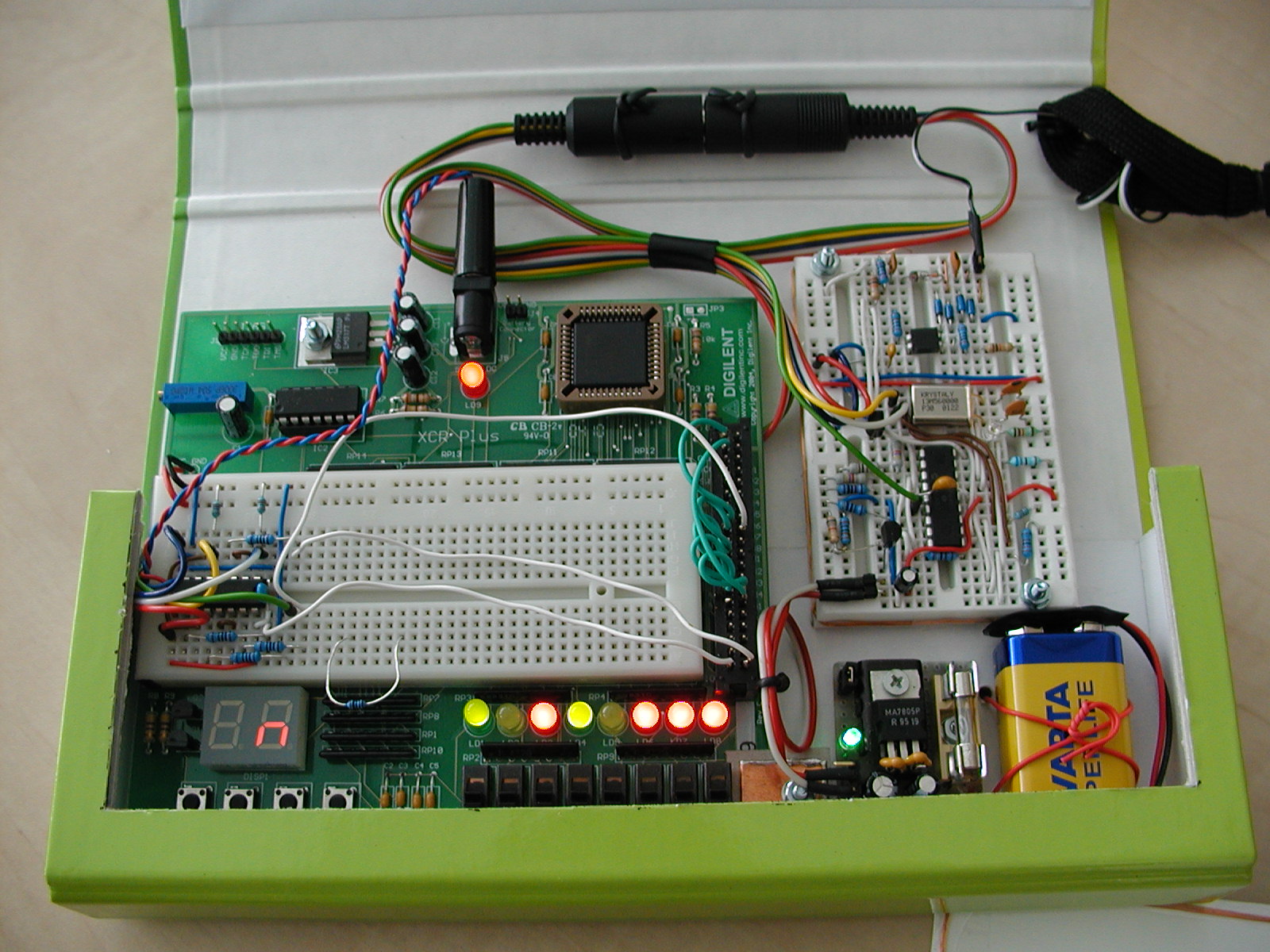
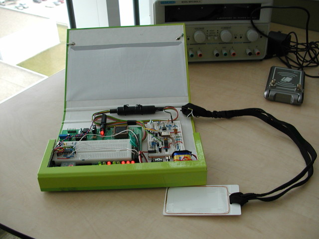
Some pictures of the whole prototype design can be found here: device detail, inner side, outer box.
ALPHA codes snapshot - just to get an idea (interconnection with CPLD can be derived from the sources).
(Ab)Using the NFC-WI/S2C interface (SAM-PicNic)
This interface is supported by several NFC front ends of NXP, mainly by the PN511 and PN512. Note that these chips are also embedded in the PN531, PN532, and PN533 controllers, since those devices are in fact composed of PN511 (or PN512) plus certain 80C51-based microcontroller core. The NFC-WI/S2C interface main purpose is to allow using the core analog Tx/Rx path for attaching the so-called Secure Module (SAM). The Secure Module can be, for instance, a somehow stripped MIFARE Classic chip (only its digital part is used).
The interface provides mainly the following five signals: power source/reference, GND, SIGOUT, SIGIN, and SIC_CLK.
The SIGOUT is an output providing modified Miller encoded data (the particular analog signal appearance depends on the particular registry configuration of the controller). The SIGIN is an input expecting Manchester coded signal with the subcarrier of 847.5 kHz (modulation signal of the transponder). The SIC_CLK provides recovered basic carrier signal of 13.56 MHz. Some other signals can be added to this interface, provided these are useful for the specific purpose. For instance, there is the CLAD signal allowing the SAM to inform the controller about start/end of the SAM RF-activity. Details can be found in the technical documentation of NXP. It can be obtained from NXP under NDA. In time of writing this notice, however, a copy of it appeared in the doc lib at www.proxmark.org.
The idea of attaching the PicNic is that simple:
- use SIGOUT in place of the antenna/demodulator output
- use SIGIN in place of MOSFET load modulator input
- use SIC_CLK as a clock source for the PIC16F648A (as it supports external clock signal allowing even the DC idle state!); yes(!) – the choice of designing the PicNic firmware as for the PIC having the clock signal the same as the RF basic carrier finally pays off here.
The main benefits of this setup should be:
- much better timing synchronization of the PicNic Rx and Tx (mainly the Tx-after-RX frame delay)
- possibility to simply “implant” PicNic into existing NFC devices; this could allow using existing antenna and low-level analog design as well as hiding the PicNic into, for instance, an NFC equipped mobile phone etc.
Current status of the project:
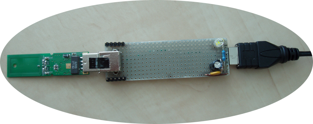
- prepare a demo board for SAM-PicNic experiments: OK
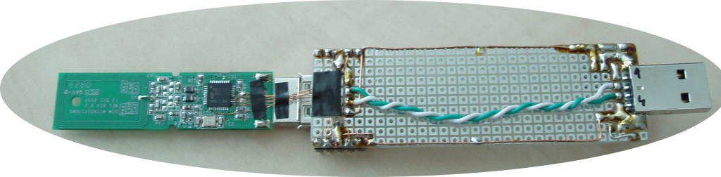
It is based on SCL3710 dongle. The interesting signals of PN531 have been drawn outside the original PCB layout. Cf. overall demo board design or SCL3710 interconnection details. The SCL3710 is driven by the libnfc library via USB channel.
- research the interconnection details: to be done (basing on the demo board measurements)
- redesign PicNic fw (minor changes are expected): to be done
- verify the real PicNic implantation: to be done
SW modules
FakeUID 1.3.2 – emulator of ISO14443A anticollison handshake for 4 bytes long UID. Certain support for data gathering for MIFARE Classic cryptanalysis is also added (see comments in the source code).
FakeUID 1.4-beta – supports ISO14443A UID of all lengths (4/7/10 bytes) and presents a redesigned Tx synchronization to allow easier application protocol extension (see comments in the source code).
FakeUID 1.4 – final version, minor changes done and some bugs corrected.
FakeUID 1.5-beta – adds a better support for the DESFire emulation. Allows capturing of terminal response for the Authenticate command. This enables offline key guessing attacks. Furthermore, it adds support for the R(NAK) – R(ACK) ping-pong which is used by some readers (e.g. CardMan 5321) to check the presence of a transponder in the terminal field. The ATS support is added as well.
FakeUID 1.5-beta OpenCard Special Edition – the exact experimental version employed for OpenCard partial emulation in applications relaying only on static transponder data (mainly UID). Surprisingly, such applications were already found! This firmware was used to show that building security of RFID applications on UID-only approach is really very, very bad idea. The whole story (in Czech) is captured here. Some technical details were discussed in this lecture (CZ).
Recommended reading
[1] Finkenzeller K.: RFID Handbook, John Wiley & Sons Ltd., 2nd edition, 2004
[2] Lee, Y.: Antenna Circuit Design for RFID Applications, Microchip Tech. Inc., 2003
[3] PIC16F627A/628A/648A Data Sheet, Microchip Tech. Inc., 2007